Semiconductors and silicon wafers have become integral components of our lives at this point. They’re everywhere, generally hidden from view, quietly making the lives we’ve come to rely on possible. They’re in phones, computers, appliances, vehicles, gaming systems, electronic toys, and countless other items everyone takes for granted these days. They’re going to become more common in the future.
Taking a Closer Look at Semiconductor Manufacturing
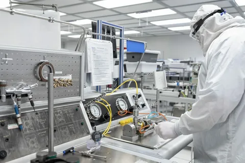
Though people don’t usually see the semiconductors in their devices and appliances firsthand, they certainly see what they’re capable of doing. These powerful and versatile components make life easier, more entertaining, and more convenient. Quite a bit of effort and engineering go into silicon wafer processing. Take a closer look at the steps involved in the manufacturing process.
Creating Silicon Ingots
It all begins with creating large, cylindrical ingots of highly purified silicon. This is done by melting silicon crystals at high temperatures in a specially designed furnace. Melted silicon is then cooled and formed into a solid cylinder known as an ingot. That paves the way for the steps to follow.
Wafer Slicing silicon
After silicon is formed into an ingot, it needs to be divided into slices that are usually about 0.7 millimeters thick. This is done with a diamond-tipped saw. It’s capable of cutting extremely thin slices without damaging the silicon. That’s important because silicon wafers need to be precise and perfect for them to work properly in the next processing stages.
Wafer Polishing
From there, silicon wafers need to be polished. They go through equipment that grinds, buffs, and etches them until they’re perfectly flat, uniform, and smooth. Even a single microscopic imperfection on a wafer’s surface could cause problems down the line. Polishing eliminates any blemishes that might remain on wafers after they’re cut.
Oxidation
Following the polishing process, silicon wafers need to be oxidized. That involves heating them to over 1,800 degrees Fahrenheit in a specially designed oven that simultaneously introduces oxygen into the mix. This process of heating and oxygen exposure creates a thin layer of silicon dioxide on the surface of the wafers.
Photolithography
Photolithography entails coating a wafer with a light-sensitive chemical. Then, manufacturers place a template on the wafer and expose it to ultraviolet light to imprint a pattern onto its surface. That determines where different components will be installed on the wafer. While the wafer is exposed to ultraviolet light, materials on its surface are either protected by the template or removed to leave behind the pattern.
Etching
Then, silicon wafers go through an etching process. Through either wet or dry etching techniques, parts of the oxidized layer created earlier is removed. That exposes areas of raw silicon for further processing.
Doping
Doping involves introducing highly controlled impurities to the surface of silicon wafers. That prepares the wafers for the components that’ll be installed on them and modifies their electrical conductivity as needed. It’s important to note that several photolithography, etching, and doping steps are needed to fully build circuits and other components on a wafer.
From Raw Materials to Essential Components
Silicon wafers start out as a hard, metallic raw mineral. That material needs to be processed and purified to be used as a semiconductor. Several steps go into creating the finished product, including cutting, polishing, oxidation, photolithography, etching, and doping. In-depth quality testing is also required to ensure the finished product is up to par. All those steps make electronics, and many of the modern conveniences we’ve come to rely on, possible.